Novafiber
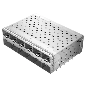
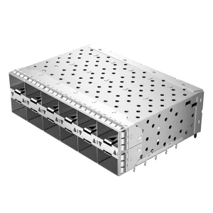
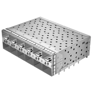
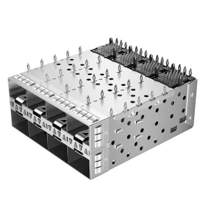
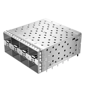
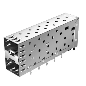
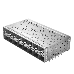
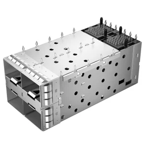
Technical Deep Dive: The Mechanics and High-Frequency Characteristics of 2xN Stacked SFP Cages
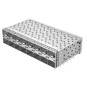
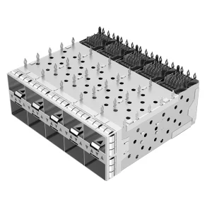
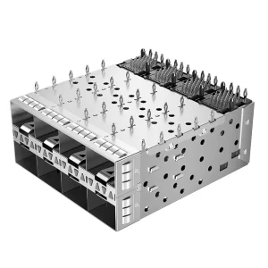
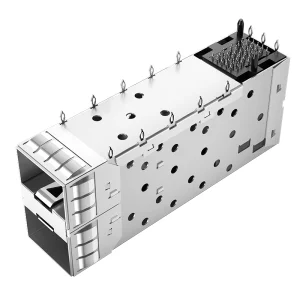
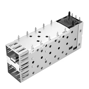
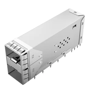
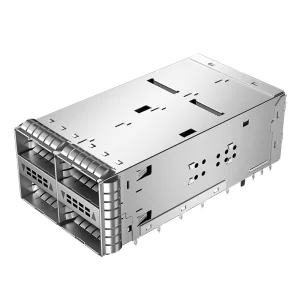
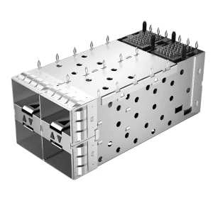
In the rapidly evolving landscape of high-performance computing, enterprise routing, and data center switching, space utilization on the printed circuit board (PCB) is a major design constraint. The 2xN stacked port configuration has emerged as the definitive solution for high-density I/O interfaces. By stacking two rows of Small Form-factor Pluggable (SFP/SFP+/SFP28) modules vertically, system designers can double the port density along the card edge without increasing the linear board footprint.
However, stacking two high-speed transceiver interfaces vertically introduces substantial engineering challenges. These include maintaining signal integrity at data rates reaching 28 Gbps per channel, mitigating electromagnetic interference (EMI) leakage through the card-edge panel, and managing thermal dissipation from adjacent, high-heat modules. As a leading manufacturer of interconnect solutions, we specialize in addressing these constraints through advanced material science, precision press-fit geometry, and robust shielding design.
Signal Integrity and Impedance Control
Operating at data rates specified by SFP+ (10 Gbps) and SFP28 (28 Gbps) requires meticulous routing and internal connector design to prevent insertion loss, crosstalk, and impedance mismatches. The internal contact structure of a stacked 2xN cage is characterized by varying pin lengths between the upper and lower ports. Left uncompensated, this difference in physical trace length would lead to timing skew and phase mismatches.
Our stacked cages employ precision-molded internal connectors with specialized pin geometry. Through advanced 3D electromagnetic field simulations, we optimize the pin shapes to guarantee consistent 100-ohm differential impedance across all paths. Crucially, this mitigates near-end crosstalk (NEXT) and far-end crosstalk (FEXT) between the vertically aligned ports, ensuring clean eye diagrams even during simultaneous transmission across all 2xN channels.
Electromagnetic Interference (EMI) Mitigation
At high frequencies, the opening of a port cage acts as an aperture for electromagnetic radiation. If not properly shielded, high-frequency noise from the ASIC or transceiver modules can leak out, failing strict FCC or CISPR EMI compatibility standards. Stacked cages are particularly susceptible to this issue due to their double-height profile.
To achieve class-leading EMI suppression, our cages utilize dual-shielding topologies:
- BeCu (Beryllium Copper) EMI Spring Fingers: Positioned around the port openings to establish low-impedance ground paths with the chassis panel. Beryllium copper retains its spring properties under long-term mechanical stress, preventing degradation after repeated insertion cycles.
- Conductive Elastomeric Gaskets: Selected for ultra-high-frequency applications, providing highly compliant, continuous grounding along the interface gap.
- Advanced Press-fit Compliant Pins: Strategically distributed across the cage body to anchor the shield directly into the PCB ground planes, shortening the EMI return path.
Global Commercial and Industrial Landscape of 2xN Stacked Port Technology
The global demand for high-density stacked interconnects is primarily driven by three macroeconomic trends: the deployment of 5G telecommunication networks, the exponential growth of artificial intelligence (AI) clusters, and the rapid expansion of hyper-scale cloud computing facilities.
Historically, network switch designs relied on single-row (1xN) cages. However, as modern AI training models demand massive parallel data transfers, standard rack space has become highly constrained. A standard 1U switch using a 1x16 SFP layout is limited in throughput; transitioning to a 2x16 or 2x8 configuration allows systems to scale bandwidth density exponentially.
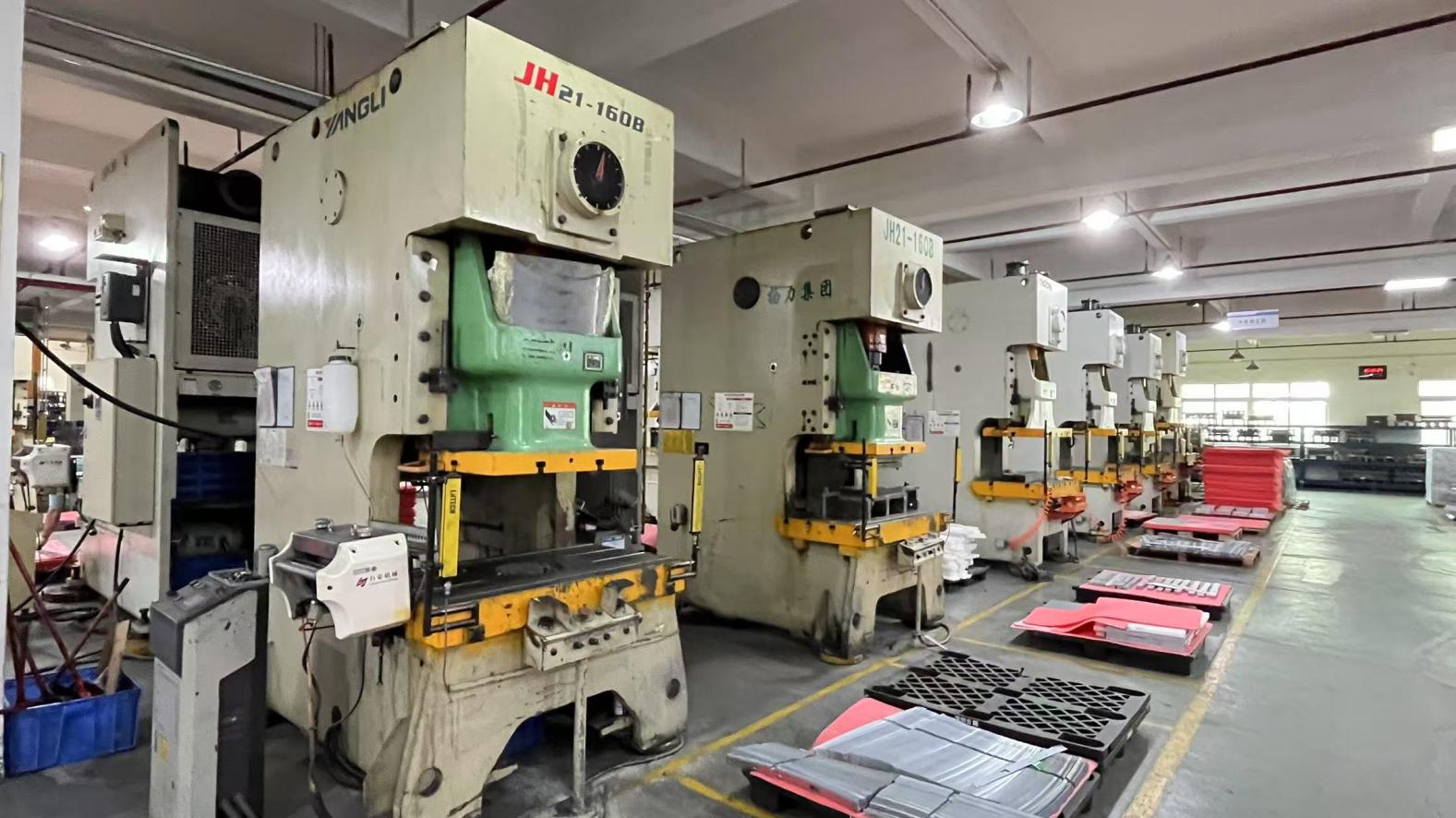
Geographically, the manufacturing ecosystem for SFP components relies on precise, automated stamping and plating facilities. The high-speed interconnect market requires strategic regional distribution to ensure supply chain resilience. Through our network of over 1,200 supply chain partners, we ensure a steady, reliable supply of high-grade copper alloys, specialized high-temperature plastics, and lightpipe plastics, providing global manufacturers with dependable OEM and ODM support.
Novafiber Communications Co., Ltd. — Manufacturing Capabilities & Trustworthy E-E-A-T Profile
Established in 2016, Novafiber Communications Co., Ltd. has spent the last 9 years positioning itself as a premier provider of high-speed fiber optic communication modules and mechanical interconnect solutions. Backed by 7 years of robust export operations, we serve system integrators and telecommunication equipment manufacturers across North America, Europe, Southeast Asia, and the Middle East.
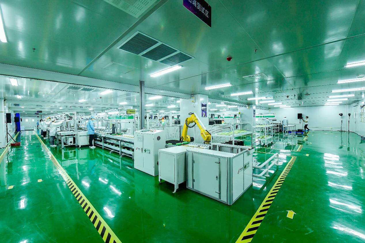
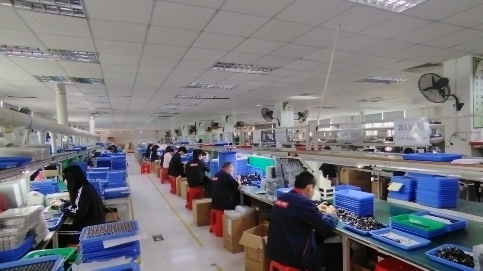
Our dedicated, high-precision assembly and R&D facility covers 420 square meters, focusing on prototype validation, advanced physical testing, and high-precision assembly. To support massive manufacturing scaling, we leverage our expansive supply network, producing high-reliability components that meet international standards.
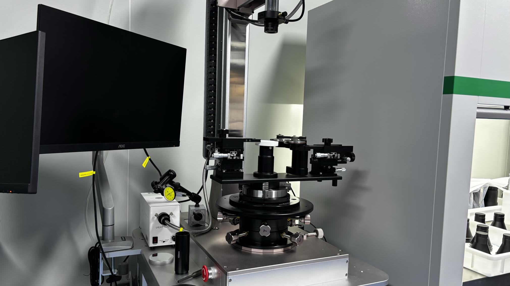
Quality is at the core of our operations. With 65 dedicated quality inspection personnel, we employ rigorous testing procedures at every stage of production. This includes automated optical inspection (AOI), X-ray plating thickness measurements, environmental stress screening (ESS), and 100% functional signal-integrity validation. All of our connectors and cages comply with IPC standards, ensuring mechanical and electrical alignment with Multi-Source Agreements (MSA) and Telcordia specifications.
Advanced R&D and Customization Focus
Innovation drives our business. Our R&D team comprises 180 experienced engineers who develop mechanical and optical technologies to stay ahead of market demands. Over the past year alone, Novafiber introduced 320 new products, ranging from standard SFP+ cages to advanced 800G optical components. We offer comprehensive OEM/ODM customization services, including custom lightpipe configurations, optimized press-fit pin layouts, modified EMI spring profiles, and tailored packaging to fit automated board assembly processes.