Novafiber Communications Co., Ltd. is a leading, high-reliability optical transceiver manufacturer and system engineering specialist catering to global data centers, cloud infrastructure providers, telecom carriers, and enterprise network integrators. Operating since 2016, Novafiber has pioneered cutting-edge optical link development and high-frequency magnetics production.
With over 9 years of industry experience and 7 years of direct export operations, we serve tier-1 networking infrastructure clients across North America, Europe, Southeast Asia, and the Middle East. Headquartered in a dedicated, high-density precision laboratory facility spanning 420㎡, Novafiber optimizes space efficiency with class-10,000 cleanrooms and advanced automated testing rigs. Backed by 1,200+ partner components suppliers, we maintain a robust supply chain configuration that guarantees continuity of supply, regardless of dynamic global semiconductor market conditions.
The global optical communications industry relies heavily on China's massive optical supply chain infrastructure. Within this critical hub, Novafiber leverages an end-to-end ecosystem of raw material vendors, semiconductor package houses, substrate fabrication foundries, and automated assembly partners. Our capability to source premium TO-cans, high-frequency printed circuit boards (PCBs), and opto-electronic components locally ensures unprecedented agility and pricing efficiency.
With 1,200+ localized suppliers, we bypass global raw material bottlenecks. We secure high-performance lasers (DFB, EML, VCSEL) and photodetectors (PIN, APD) at pre-allocated volumes to ensure continuous manufacturing pipelines.
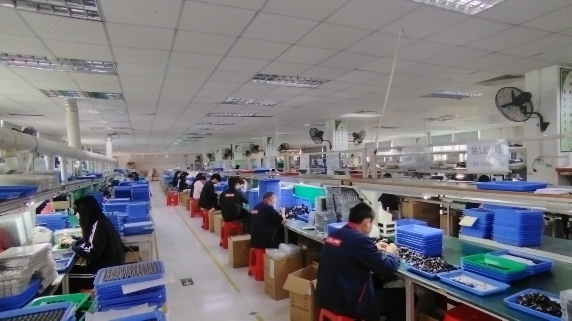
By utilizing advanced SMT machinery and automated sub-micron optical alignment systems, we maintain defect rates below 100 DPPM (Defective Parts Per Million) while dramatically scaling output capacity.
With 180 expert hardware, software, and mechanical engineers on staff, Novafiber can cycle a custom protocol design or a non-standard form factor from concept to validated prototype within just 15 days.
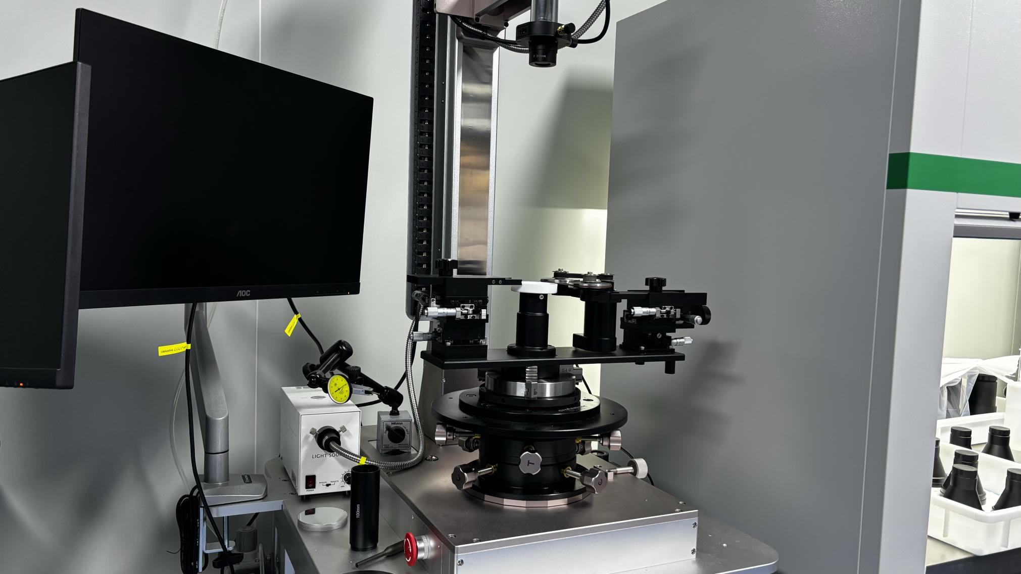
Our 420㎡ state-of-the-art cleanroom facility houses world-class micro-assembly, packaging, and optical parameter testing equipment.


Network architects and procurement directors from telecom operators, global enterprise data centers, and web-scale cloud services face distinct technical and commercial hurdles when sourcing optical transceiver modules. Understanding these pain points forms the foundation of our engineering services.
At Novafiber, we employ a dedicated workforce of 65 quality inspection personnel. Every single component must satisfy IPC standards and undergo automated optical testing (AOI) alongside Environmental Stress Screening (ESS). Our quality framework includes:
Hardware compatibility is a non-negotiable procurement standard. The Novafiber R&D team runs firmware adaptation and protocol modification tests to guarantee 100% interoperability with major OEM networking environments including Cisco, Arista, Juniper, Dell, and HPE.
Operating globally requires strict adherence to international trade guidelines, environmental laws, and optical safety mandates. Novafiber provides extensive support services to verify compliance across all jurisdictions we serve:
Our manufacturing facilities adhere strictly to RoHS (Restriction of Hazardous Substances) and REACH standards. We implement lead-free soldering and utilize non-hazardous plastics and adhesives throughout assembly, ensuring safe end-of-life component recycling.
Novafiber transceivers carry CE, FCC Part 15, and TUV markings. All active optical components conform to Class 1 Laser Safety regulations (IEC 60825-1 / FDA CDRH), ensuring complete user and installer safety under normal operation.
To bridge global time zones, we offer direct Field Application Engineering (FAE) support. We assist engineering teams with protocol setup, hardware debug, and network troubleshooting in North America, Europe, and Asia.
As data demands expand exponentially with artificial intelligence (AI), machine learning (ML), and 5G deployment, optical transceivers are undergoing structural transformations. Our R&D division (releasing 320 new products over the past year) is active in several key technical areas:
By mounting optical engines directly onto the same substrate as the network switch ASIC, CPO minimizes electrical trace distances. This leads to dramatic reductions in power consumption and signal attenuation, replacing traditional pluggable optics in hyperscale AI training clusters.
Silicon Photonics integrates optical components onto a single silicon chip using standard CMOS manufacturing lines. This helps lower unit cost, improve thermal performance, and maximize channel density for next-generation 800G and 1.6T systems.
LPO eliminates the internal DSP (Digital Signal Processor) inside the transceiver module, relying instead on the switch ASIC's host SerDes for signal conditioning. This drops transceiver power draw by up to 50% and minimizes latency to nanosecond levels.
Our products are deployed in various industries, demonstrating the versatility of our optical and magnetic components:
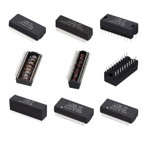
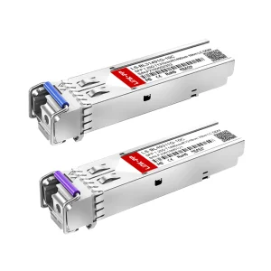
 Novafiber