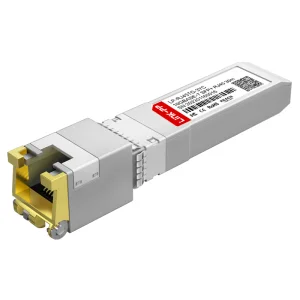
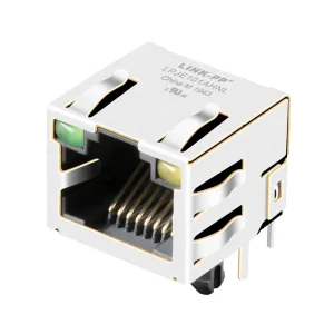
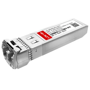
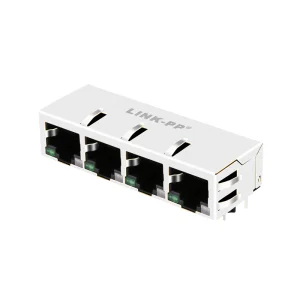
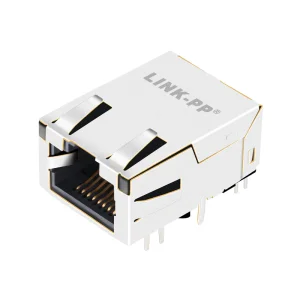
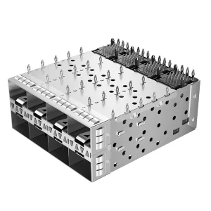
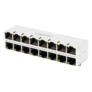
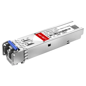
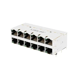
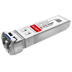
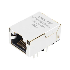
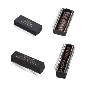
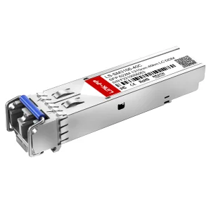
Engineered for low signal loss, exceptional electromagnetic interference (EMI) protection, and high durability across harsh enterprise environments.
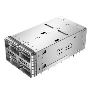
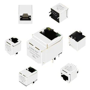
As next-generation data centers, enterprise networks, and cloud compute nodes transition toward multi-gigabit and terabit architectures, the reliability of physical-layer (PHY) connectivity remains the ultimate benchmark of system uptime. Wired network connectors, ranging from specialized multi-port stacked RJ45 magnetic assemblies to high-density zQSFP+ and SFP+ cage interfaces, serve as the foundational bridges for critical data transport. Signal integrity, thermal management, and robust electromagnetic shielding (EMI) are no longer ancillary considerations; they are decisive metrics that govern the performance boundaries of modern networking equipment.
At Novafiber Communications Co., Ltd., we bridge the gap between high-speed physical engineering and scalable manufacturing. By providing fully compliant, pin-compatible, and drop-in OEM alternatives (compatible with leaders like TE Connectivity, Cisco, Molex, and Würth Elektronik), we enable global network system integrators, telecom operators, and data center engineers to optimize their hardware design while retaining absolute economic control over their physical-layer procurement.
Advanced shielding fingers and multi-point grounding tabs minimize Near-End Crosstalk (NEXT) and Far-End Crosstalk (FEXT) in high-speed, high-density applications.
Integrated copper-alloy matrix designs combined with strategically placed lightpipes and heat sink integrations maximize heat dissipation in high-density port configurations.
100% compliance with IEEE 802.3 ethernet parameters, SFF-8431, SFF-8432 MSA specifications, and strict compliance with global RoHS, REACH, and UL regulations.
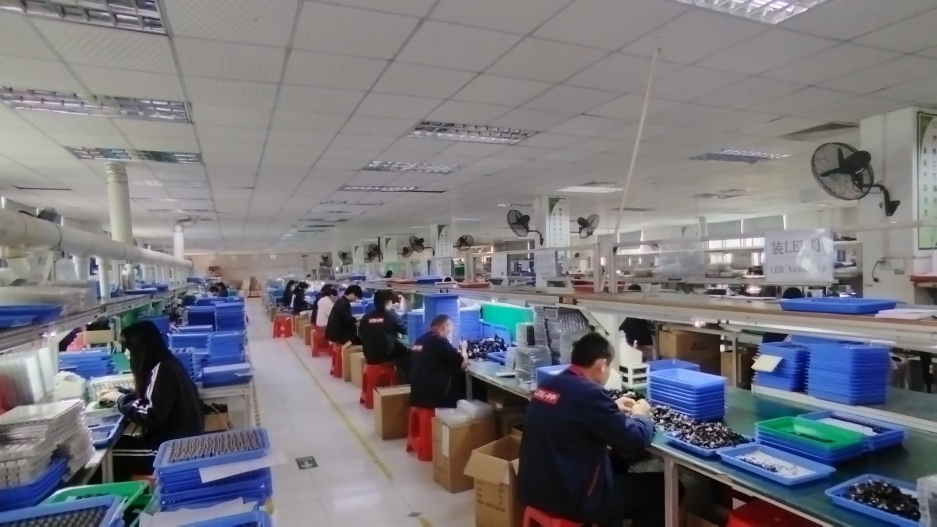
The global dominance of China-based interconnect manufacturing is driven by a deep convergence of technical infrastructure, localized material supply webs, and highly automated assembly processes. China's network connector clusters—predominantly concentrated in Guangdong (Shenzhen/Dongguan) and Zhejiang regions—provide an unmatched ecosystem that spans high-precision stamping dies, selective gold-plating chemical engineering, precision plastic injection molding, and highly coordinated logistics networks.
This localized synergy allows manufacturers like Novafiber Communications to execute rapid engineering prototyping (from 3D CAD design to functional press-fit evaluation samples within days) and transition directly into scale-up mass production. With an expansive framework containing more than 1,200 supply chain partners, we eliminate bottlenecks associated with raw materials, copper-alloy alloys, high-performance LCP (Liquid Crystal Polymer) plastics, and electronic packaging components. The result is a highly resilient delivery matrix that protects global operations from unexpected raw material shortages and geopolitically induced shipping delays.
A glimpse into our manufacturing scale, high-precision assembly lines, automated optical inspection, and reliability engineering labs.

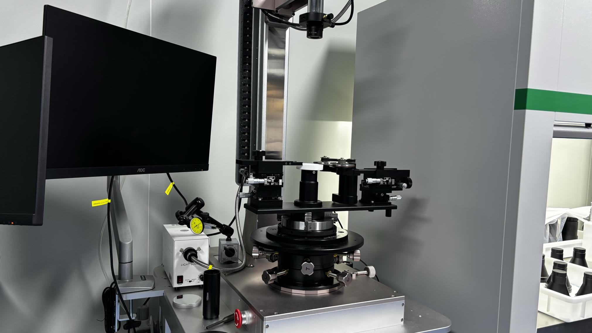
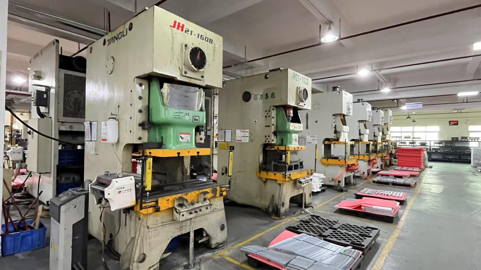
Off-the-shelf connectors often fail to address the specific structural boundaries of specialized networking motherboards, ruggedized industrial systems, or unique system-on-chip (SoC) interface requirements. To mitigate this risk, Novafiber offers highly flexible and structured OEM/ODM customization services backed by a robust engineering team of 180 specialists. Whether you require selective gold plating thicknesses (ranging from flash gold up to 50 micro-inches for extreme industrial conditions), alternative LED color combinations (green, yellow, orange, blue, or bi-color), or customized electromagnetic shielding layout parameters, our engineering labs design, model, and tool solutions that conform exactly to your system requirements.
Operating a global telecommunications network requires adherence to strict regulatory guidelines and high logistics synchronization. We ensure that every batch of network connectors, SFP cages, and optical transceivers leaving our facilities complies fully with RoHS and REACH environmental standards, guaranteeing clean, lead-free products. Furthermore, we recognize that hardware integration issues demand immediate, expert resolution. Through our network of regional partners and remote engineering support channels, we deliver prompt localized technical support, assisting system designers with PCB trace optimization, footprint layouts, eye-diagram troubleshooting, and compliance validation. This level of technical oversight ensures smooth product development lifecycles from concept to mass production.
To secure consistent performance across thousands of units, our 65 dedicated quality inspection professionals employ a multi-layered testing regimen aligned with IPC standards. This includes:
Answering the most critical technical questions asked by hardware engineers, network architects, and procurement managers.
Designed for carrier-grade applications, heavy enterprise routing switches, and high-capacity fiber termination boxes.
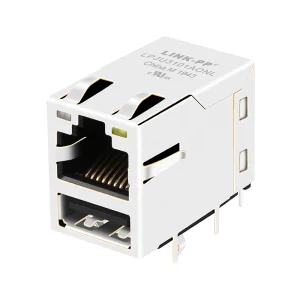
 Novafiber